Speed and Resiliency Still Rule
Key Takeaways:
- Speed-to-market remains the key driver of small-to-mid-size chip manufacturing facilities projects, with companies under pressure to outpace competitors and meet CHIPS Act funding deadlines.
- Global energy price volatility and supply chain issues are forcing chip fabrication plant (fab) owners to double down on resiliency strategies during design and construction.
- While less contentious than data center projects, chip fabs face community pushback and permitting challenges that can slow down project schedules.
- Owners must prioritize adaptability when planning their chip fab facilities, so that operations can shift to accommodate new technologies.

Q: How do mid-size semiconductor facilities differ from the mega fabs that dominate the news cycle?
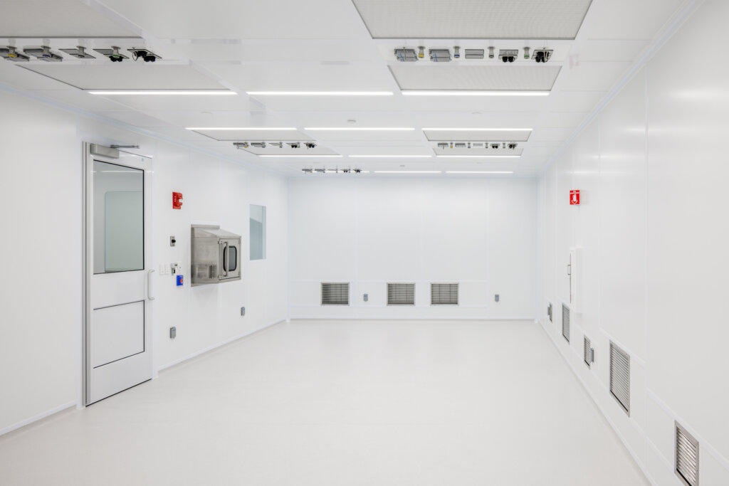
A: The core technology is the same, but the difference is the purpose the facility serves. Mid-scale fabs tend to support more specialized applications—pilot lines, targeted manufacturing, controlled environments. They still require sophisticated cleanrooms and infrastructure, but they’re designed around precision and adaptability rather than sheer production capacity.
In many cases, these facilities are more constrained. Owners are managing tighter budgets and smaller footprints, while still needing to deliver a highly technical environment. That creates a different design challenge.
We’ve seen this throughout our work. Even when we worked with IBM in the 1990s, which was a major player in the industry, a number of those projects were targeted facilities rather than very large campuses.